Glass PCB
Nanotronix has developed a embedded side wrap patterning method for TFT composite structures(multi-metal layers patterns on glass) for micro LEDs, and has various experiences in glass surface patterning, such as transparent glass signage and CIS patterning on a pan-out type glass substrate base.
It also holds more than 10 related patents.
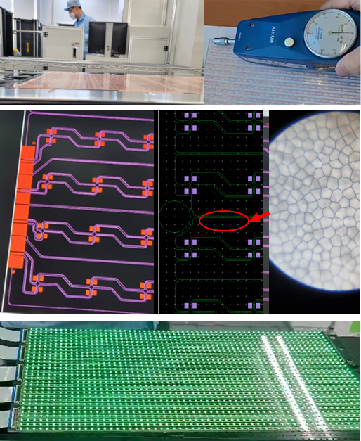
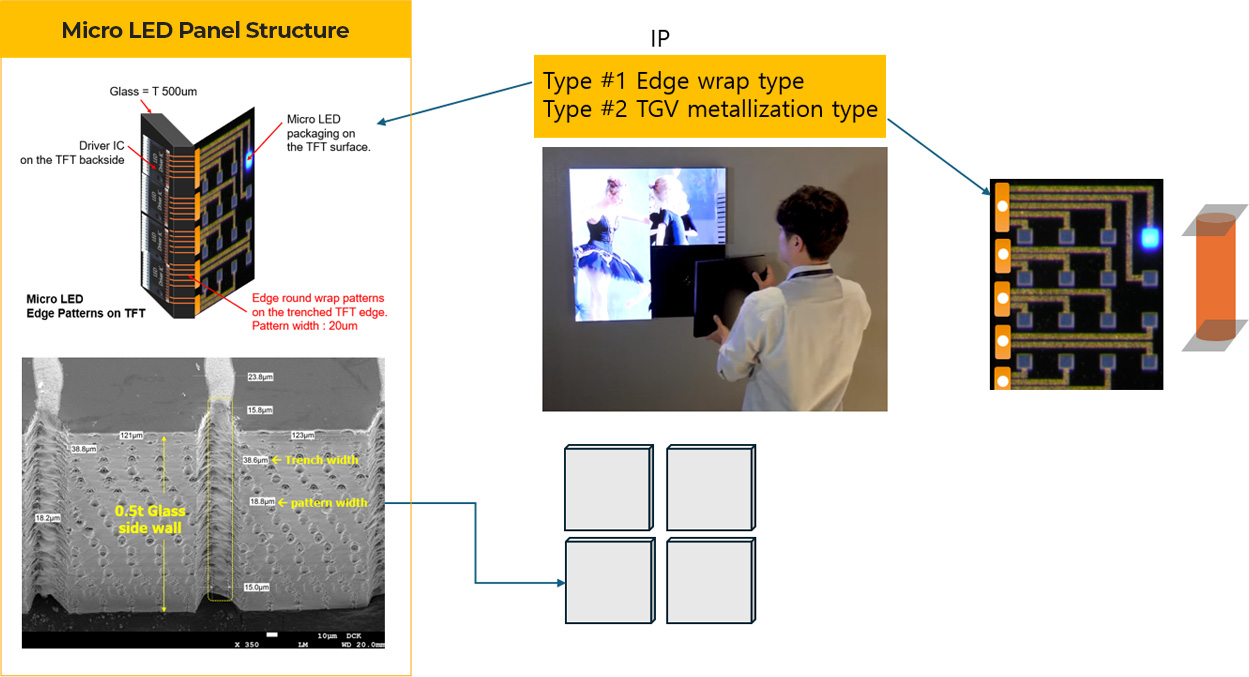
Micro LED : TFT edge wrap patterns (Embedded Patterns)
2D Patterning on glass (FO-CIS & Glass signage)
- 1. Substrate : Glass
- 2. Micro patterning size : 10x10mm to 250 x 500mm
- 3. Applied technologies : plating, sputtering and etching
- 4. Pattern width : 5~100um
- 5. Application(ex)
- 1) CIS chip pan-out patterns(2016)
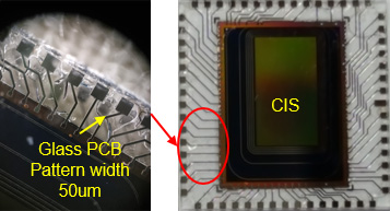
- 2) Glass PCB(LED pad) : Straight, Mesh.(2022)
- 1) CIS chip pan-out patterns(2016)